- 您现在的位置:买卖IC网 > Sheet目录484 > NOIH2SM1000S-HHC (ON Semiconductor)IC SPACE IMAGE SENSOR 84-JLCC
NOIH2SM1000A
DETAILED INFORMATION
Deviations from Generic Specification
Lot acceptance and screening are based on ESCC 9020
issue 2. See Lot Acceptance and Screening on page 6 for
more information.
Mechanical Requirements
Dimension Check
The dimensions of the components specified here is
checked and must comply with the specifications and the
tolerances indicated in Figure 4 on page 25
Geometrical Characteristics
The geometrical characteristics of the components
specified here is checked and must comply with the
specifications and tolerances given in Figure 4 on page 25
and Figure 3 on page 10
Weight
The maximum weight of the components specified here is
specified in Table 14 on page 10
Materials and Finishes
The materials and finishes is as specified in this document.
Where a definite material is not specified, a material which
enables the components to meet the performance
requirements of this specification must be used. See Note 2.
Case
The case is hermetically sealed and must have a ceramic
body and a glass window.
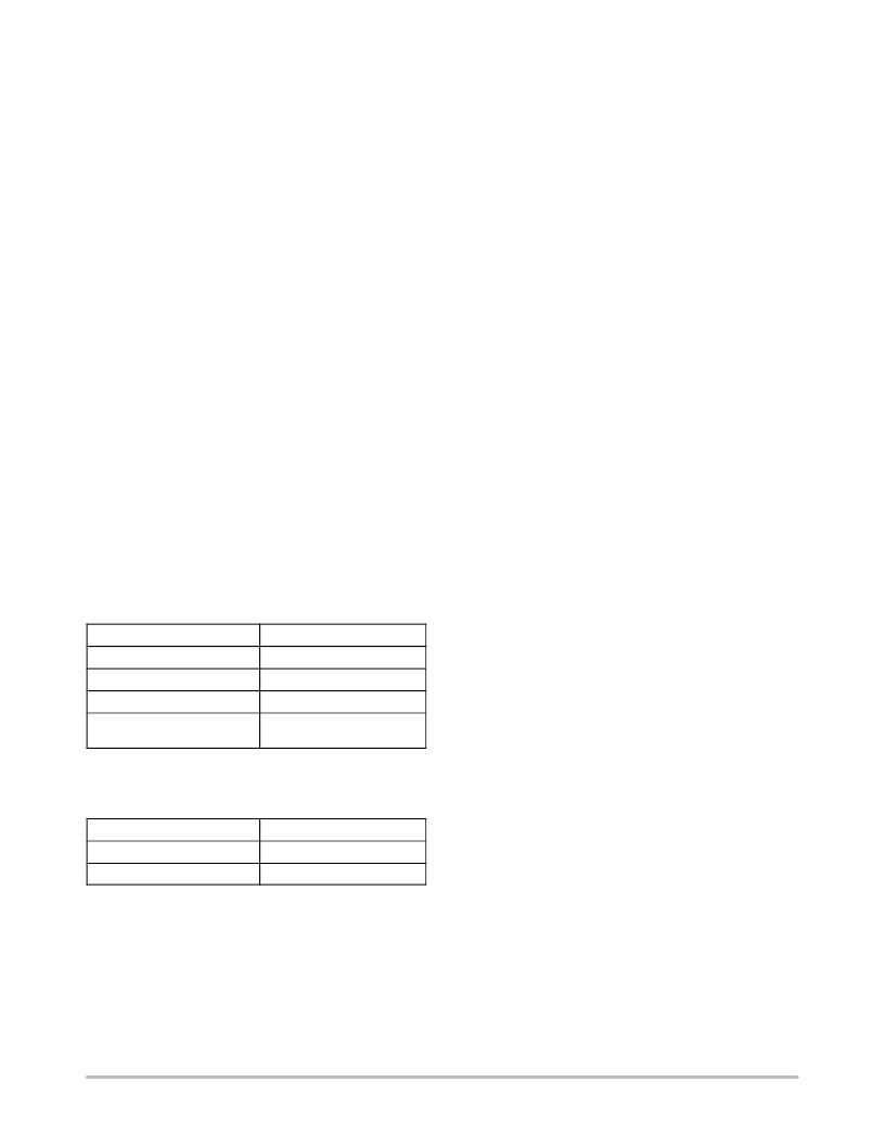
Table 3. CASE
Type JLCC ? 84
Material Black Alumina BA ? 914
Thermal expansion coefficient 7.6 x 10 ? 6/K
Hermeticity < 5 x 10 ? 7 atms. cm 3 /s
Thermal resistance 3.633 ° C/W
(Junction to case)
Lead Material and Finish
Table 4. LEAD MATERIAL AND FINISH
The anti reflective coating has a reflection coefficient less
than 1.3% absolute and less than 0.8% on average, over a
bandwidth from 440 nm to 1100 nm.
Level 2 versus Level 1 differences
HAS2 Level 2 devices are differing from Level 1 devices
in Lot Acceptance and Screening on page 6
? 100% screening is applied with burn-in limited to 168 h
instead of 240 h as for Level 1.
? Assembly process is based on ESA qualified process
(same procedures and materials)
? Devices will be fully tested at room temperature,
electrical testing at 85 degrees is limited to power
consumption measurements only.
? X/Y dye placement is relaxed to +/- 200 m m.
? Mismatching between odd and even columns in Direct
Readout is allowed but shall stay in the limit of
127 LSB.
? The defect and particles specification will be the same
as for the Engineering Model - NOIH2SM1000A-HHC
– with the exception of the defective columns which are
not allowed in the Level 2 devices. Refer to Table 10
“Type Variant Summary” on page 9.
? Endurance testing during wafer LAT is limited to a
1000 h burn in instead of 2000 h and will be performed
on 3 un- screened parts instead of 6.
? Prior to endurance testing and total dose testing, a
stabilization bake of 48 hrs, followed by a 168 hrs
burn-in, shall be performed.
? During wafer LAT, the Electro-optical measurements is
limited on 2 parts (1 from endurance testing and 1 from
radiation testing) instead of 6.
? For each assembly batch (manufacturing-lot), 2
screened devices will be made available for a DPA test.
An assembly batch is defined as a group of parts which
have been assembled within a time window of less than
one week. The DPA devices can be rejected devices
(glass lid cosmetic defects, electrical defects, … ) but has
to be screened through the same thermal steps as the
Lead Material
1e Finish
2 nd Finish
KOVAR
Nickel, min 2 m m
Gold, min 1.5 m m
HAS2 “level2”. The DPA test will be carried out by
ON Semiconductor as a customer courtesy.
Prior to DPA testing, the following tests are performed:
Solderability and Resistance to Solvents (marking
permeability).
Window
The window material is a BK7G18 glass lid with
anti-reflective coating applied on both sides.
The optical quality of the glass must have the
specifications in Table 15 on page 11.
NOTE: As the glass lid removal is a best effort activity,
the DPA test cannot be 100% guaranteed.
? Pictures and defect maps are not included in the data
pack, but will be made available upon request.
? Assembly lot acceptance testing is not performed.
http://onsemi.com
3
发布紧急采购,3分钟左右您将得到回复。
相关PDF资料
NOII5SM1300A-QDC
SENSOR IMAGE MONO CMOS 84-LCC
NOIL1SC4000A-GDC
IC IMAGE SENSOR 4MP 127-PGA
NOIL1SE3000A-GDC
IC IMAGE SENSOR 3MP 369-PGA
NOIL1SM0300A-WWC
IC IMAGE SENSOR LUPA300 48LLC
NOIL2SC1300A-GDC
IC IMAGE SENSOR LUPA1300 168PGA
NOIV1SE025KA-GDC
IC IMAGE SENSOR 25MP 355PGA
NP100P04PDG-E1-AY
MOSFET P-CH -40V MP-25ZP/TO-263
NP100P04PLG-E1-AY
MOSFET P-CH -40V MP-25ZP/TO-263
相关代理商/技术参数
NOII4SM1300A-QDC
功能描述:SENSOR IMAGE MONO CMOS 84-LCC RoHS:否 类别:传感器,转换器 >> 图像,相机 系列:- 标准包装:480 系列:- 象素大小:6.7µm x 6.7µm 有源象素阵列:768H x 488V 每秒帧数:52 电源电压:3.3V 类型:CMOS 成像 封装/外壳:48-QFP 供应商设备封装:48-QFP 包装:托盘 请注意:* 配用:4H2105-ND - HEADBOARD FOR KAC-004014H2104-ND - KIT EVAL FOR KAC-00401 其它名称:4H20954H2095-NDKAC-00401-CBC-LB-A0
NOII4SM1300A-QWC
功能描述:SENSOR IMAGE MONO CMOS 84-LCC RoHS:否 类别:传感器,转换器 >> 图像,相机 系列:- 标准包装:480 系列:- 象素大小:6.7µm x 6.7µm 有源象素阵列:768H x 488V 每秒帧数:52 电源电压:3.3V 类型:CMOS 成像 封装/外壳:48-QFP 供应商设备封装:48-QFP 包装:托盘 请注意:* 配用:4H2105-ND - HEADBOARD FOR KAC-004014H2104-ND - KIT EVAL FOR KAC-00401 其它名称:4H20954H2095-NDKAC-00401-CBC-LB-A0
NOII4SM6600A-QDC
功能描述:图像传感器和彩色传感器 IBIS4-6600 MONO LLC68 RoHS:否 制造商:Avago Technologies 类型:Color Sensors 工作电源电压:2.5 V 封装 / 箱体: 图象大小: 颜色读出:Color 最大工作温度:+ 70 C 最小工作温度:- 25 C 封装:Reel
NOII5FM1300A-QDC
功能描述:SENSOR IMAGE 1.3MP CMOS 84-LCC RoHS:否 类别:传感器,转换器 >> 图像,相机 系列:- 标准包装:480 系列:- 象素大小:6.7µm x 6.7µm 有源象素阵列:768H x 488V 每秒帧数:52 电源电压:3.3V 类型:CMOS 成像 封装/外壳:48-QFP 供应商设备封装:48-QFP 包装:托盘 请注意:* 配用:4H2105-ND - HEADBOARD FOR KAC-004014H2104-ND - KIT EVAL FOR KAC-00401 其它名称:4H20954H2095-NDKAC-00401-CBC-LB-A0
NOII5SC1300A-QDC
功能描述:SENSOR IMAGE COLOR CMOS 84-LCC RoHS:否 类别:传感器,转换器 >> 图像,相机 系列:- 标准包装:480 系列:- 象素大小:6.7µm x 6.7µm 有源象素阵列:768H x 488V 每秒帧数:52 电源电压:3.3V 类型:CMOS 成像 封装/外壳:48-QFP 供应商设备封装:48-QFP 包装:托盘 请注意:* 配用:4H2105-ND - HEADBOARD FOR KAC-004014H2104-ND - KIT EVAL FOR KAC-00401 其它名称:4H20954H2095-NDKAC-00401-CBC-LB-A0
NOII5SM1300A-QDC
功能描述:SENSOR IMAGE MONO CMOS 84-LCC RoHS:否 类别:传感器,转换器 >> 图像,相机 系列:- 标准包装:480 系列:- 象素大小:6.7µm x 6.7µm 有源象素阵列:768H x 488V 每秒帧数:52 电源电压:3.3V 类型:CMOS 成像 封装/外壳:48-QFP 供应商设备封装:48-QFP 包装:托盘 请注意:* 配用:4H2105-ND - HEADBOARD FOR KAC-004014H2104-ND - KIT EVAL FOR KAC-00401 其它名称:4H20954H2095-NDKAC-00401-CBC-LB-A0
NOIL1SC4000A-GDC
功能描述:IC IMAGE SENSOR 4MP 127-PGA RoHS:是 类别:传感器,转换器 >> 图像,相机 系列:* 标准包装:480 系列:- 象素大小:6.7µm x 6.7µm 有源象素阵列:768H x 488V 每秒帧数:52 电源电压:3.3V 类型:CMOS 成像 封装/外壳:48-QFP 供应商设备封装:48-QFP 包装:托盘 请注意:* 配用:4H2105-ND - HEADBOARD FOR KAC-004014H2104-ND - KIT EVAL FOR KAC-00401 其它名称:4H20954H2095-NDKAC-00401-CBC-LB-A0
NOIL1SE0300A-QDC
功能描述:SENSOR IMAGE COLOR CMOS 48-LCC RoHS:否 类别:传感器,转换器 >> 图像,相机 系列:- 标准包装:480 系列:- 象素大小:6.7µm x 6.7µm 有源象素阵列:768H x 488V 每秒帧数:52 电源电压:3.3V 类型:CMOS 成像 封装/外壳:48-QFP 供应商设备封装:48-QFP 包装:托盘 请注意:* 配用:4H2105-ND - HEADBOARD FOR KAC-004014H2104-ND - KIT EVAL FOR KAC-00401 其它名称:4H20954H2095-NDKAC-00401-CBC-LB-A0
